Description
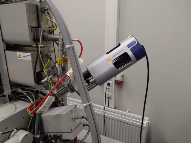 Institute of Physics at University of Tartu offers elemental analysis of wood, wood-based materials, protective coatings and other electrically non-conductive materials using the FEI NanoSEM 450 microscope. EDS tehnique determines the elemental composition of the sample surface and maps the distribution of elements. It enables the investigation of wood and coating compositions, particle identification, and comparison of materials and treatments. We use the new Oxford Instruments Ultim Max Infinity 100 mm² EDS detector and AZtec Advanced software with Feature and LayerProbe modules. When examining electrically non-conductive samples, water vapour helps neutralise electrical charging, ensuring more stable measurements.
The result is an overview of the material’s elemental composition, supporting research and development, quality control, and material comparison.
Technical parameters |
||
| Parameter | Value and unit | Additional information |
| Big sensor | 100 mm2 | A larger sensor collects more signal and significantly reduces measurement time, which is particularly important for mapping elemental distributions across a surface.
|
| Energy resolution (C Kα) | (C Kα) ≤46 eV @ 50,000 cps
(Mn Kα) ≤127 eV @ 200,000 cps |
|
| Element detection range | Be (Z=4) kuni Cf (Z=98) | Enables the detection and measurement of light elements. |
| EDS analysis | Tru-Q IQ tehnology | Tru-Q IQ is Oxford Instruments’ intelligent EDS analysis technology that automatically optimises X-ray spectrum processing and improves elemental identification and quantitative analysis accuracy. |
| Detector window | SATW (Ultra-Thin Polymer Window) | |
| Low-energy detection | Optimised for the detection of light elements. | |
| Software add-on modules | Feature | An AZtec EDS software add-on that enables the identification, analysis and classification of different sample phases, microstructural regions and particles based on their size, shape and composition. |
| Software add-on modules | LayerProbe | An AZtec EDS software add-on for analysing the composition and thickness of thin films and multilayer materials. |
Testing services include:
- Elemental analysis of electrically non-conductive samples using a scanning electron microscope
- Elemental analysis of standard samples
- Analysis and classification of particles and structures using the AZtec EDS Feature add-on module
- Determination of the composition and thickness of layered structures using the EDS system with the LayerProbe add-on module
In addition, we offer standard electron microscopy of electrically conductive and non-conductive samples.
Example of price offer
Prices depend on the nature of the samples and the complexity of the measurements required. They also vary depending on whether individual measurements or larger batches of samples are involved. The depth and complexity of the analysis are additional pricing factors. Hourly rates range from €91 to €205 + VAT and these may change in time.
To discuss your potential requirements, contact Siim Pikker at siim.pikker@ut.ee, +372 5059521